Showing posts with label Electronics. Show all posts

Sunday, April 11, 2010

Tab Electronics Guide to Understanding Electricity and Electronics


Tab Electronics Guide to Understanding Electricity and Electronics
Publisher: McGraw-Hill | Pages: 459 | 2000-07-21 | ISBN 0071360573 | PDF | 3 MB

BOOK DESCRIPTION

All-inclusive introduction to electricity and electronics. For the true beginner, there's no better introduction to electricity and electronics than TAB Electronics Guide to Understanding Electricity and Electronics , Second Edition.

Randy Slone's learn-as-you-go guide tells you how to put together a low-cost workbench and start a parts and materials inventory--including money-saving how-to's for salvaging components and buying from surplus dealers. You get plain-English explanations of electronic components-resistors, potentiometers, rheostats, and resistive characteristics-voltage, current, resistance, ac and dc, conductance, power...the laws of electricity...soldering and desoldering procedures...transistors...special-purpose diodes and optoelectronic devices...linear electronic circuits...batteries...integrated circuits...digital electronics...computers...radio and television...and much, much more. You'll also find 25 complete projects that enhance your electricity/electronics mastery, including 15 new to this edition, and appendices packed with commonly used equations, symbols, and supply sources.


Electronics Projects For Dummies


Earl Boysen, Nancy C. Muir, "Electronics Projects For Dummies"
For Dummies | 2006 | ISBN: 0470009683 | 408 pages | PDF | 12,7 MB 
BOOK DESCRIPTION

These projects are fun to build and fun to use
Make lights dance to music, play with radio remote control, or build your own metal detector

Who says the Science Fair has to end? If you love building gadgets, this book belongs on your radar. Here are complete directions for building ten cool creations that involve light, sound, or vibrations -- a weird microphone, remote control gizmos, talking toys, and more, with full parts and tools lists, safety guidelines, and wiring schematics.
Check out ten cool electronics projects, including
* Chapter 8 -- Surfing the Radio Waves (how to make your own radio)
* Chapter 9 -- Scary Pumpkins (crazy Halloween decorations that have sound, light, and movement)
* Chapter 12 -- Hitting Paydirt with an Electronic Metal Detector (a project that can pay for itself)
Discover how to
* Handle electronic components safely
* Read a circuit diagram
* Troubleshoot circuits with a multimeter
* Build light-activated gadgets
* Set up a motion detector
* Transform electromagnetic waves into sound

DOWNLOAD LINKS


DOWNLOAD FROM depositfiles.com
 
Reblog this post [with Zemanta]

Friday, April 9, 2010

DELAY TIMER PROJECT-BASIC ELECTRONICS

Introduction to Delay Timer
In this Delay Timer project, all analog parts are being used with the thyristor as a device that switches an AC Relay ON or OFF depending on the timing of the RC circuit. The input mains supply used ranges from 220VAC to 240VAC and an AC relay (220-240VAC) is used to switch a load. The load to be switched must be within the current and relay ratings. This circuit is useful for use of devices that need to be OFF for a minimum of 150 - 210 secs after a mains supply have cuts off. Devices such as compressors and halagon lamp cannot be OFF and ON repeatedly within a short period of time as it will cause damage to the devices.
The use of microcontroller based devices are not reliable in that if the power supply cuts off and came back again in a short period of time, it will reset and "forgotten" its previous state. The use of RC circuitry as a timer circuit is reliable and is not susceptible to "memory loss" as in the case of microcontroller.
If a microcontroller based solution is used, extra circuitry such as backup battery or supercapacitor need to be incorporated in order to retain the memory of the MCU and to ensure that the clock still runs even after the supply has cuts off.
This project should be handled by experienced electronics designer as its part are powered on directly from the mains supply. As all parts is "live", one may get electric shock if care is not taken when testing the circuit. Some parts may "burst" if there are some short circuit in the circuit. It is not recommended to use breadboard to test the circuit. Circuit should be tested using printed circuit board and an isolating variable transformer where the voltage is slowly ramped up from zero.
Once tested working, the components should be potted using epoxy with only the terminals exposed. All parts are potted to prevent users from touching the parts.


google_protectAndRun("ads_core.google_render_ad", google_handleError, google_rend
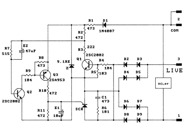
Schematic Diagram
The schematic below shows the circuit diagram of the ON delay timer. Once the mains power supply cuts off, the relay will only be able to turn ON after a period of 150 - 210 secs depending on the tolerance of the RC circuit represented by resistor R7(5.1 Mohm) and electrolytic capacitor E2(47uF). More accurate timing can be achieved by using low tolerance resistor and capacitor.
The thyristor used can be either 2P6M or MCR106-8 or equivalent parts available in the market. Relays used should have coil ratings below 1A in order not to overheat the SCR. No heatsink is required for the SCR.
At power on, there is no charge at E2, hence the transistor Q2 will be forward bias and turn ON when Q3 turn ON. Once these two transitors are ON, the SCR will turn ON as well. The use of C1 and R6 across the SCR acts as a snubber circuit to reduce the switching noise generated by the SCR when it turns OFF/ON. During the ON stage of the SCR, the capacitor E2 is charged to its maximum value. When the mains supply cuts off, the charge at capacitor E2 will cause the base of transistor Q2 to be reverse bias and cannot turn ON until almost all the charges have been discharged through resistor R7. Once the charge has been discharged (which will take around 150 - 210 secs for the values shown), transistor Q2 will be able to turn ON.
The timing of the circuit can be changed by reducing or increasing the RC values of R7 and E2.


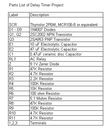
Parts List The parts list of the delay timer circuit is as shown below.


Tuesday, April 6, 2010

Electronic Timer Switch - TIMER PROJECTS

Electronic Timer Switch
This electronic timer switch project is a good project to build to simulate the presence of occupants in a house. In these days when security is becoming more of a concern when no one is at home, having this device will deter the thief from breaking in. When power up, after 60 minutes, the relay will turn ON for 100 secs, OFF for the next 100 secs, and ON again for 100 secs before OFF again for the next 60 mins. This sequence will be repeated. A device such as a lamp that is connected to the relay will turn ON and OFF according to this timing.


Schematic Diagram
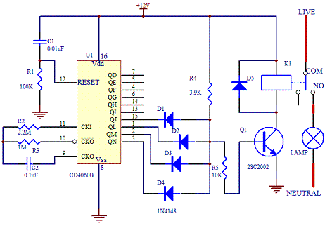
The schematic of the project is as shown below.


The core of this electronic timer switch project uses a CD4060B binary counter. The binary counter has 10 outputs and the counter are counted by configuring the oscillator. Every negative clock will trigger the counter of the IC internally.
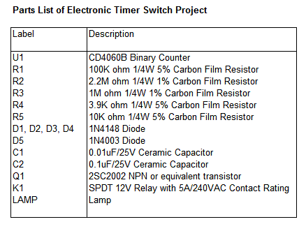
The timing of the circuit is affected by resistor R3(1M ohm) and capacitor C2(0.1uF). By connecting the four outputs in an AND configuration, the transistor Q1 will only turn ON if all the 4 outputs are in logic "1". If any of the logic is "0", the transistor will remain OFF.
For a complete cycle, the transistor will be ON twice when the output at pin 15, QJ goes to logic "1" and "0" twice when the other outputs QL, QM and QN remain at "1". When this happen, the relay K1 will switch status accordingly. The timing of the switching can be changed by changing the resistor values R2, R3 and C2. Download the data sheet of CD4060B from Texas Instrument website for more details.
Note that since the oscillator is not using crystal, the timing may not be as accurate compared to the ideal calculation. In most cases, fine tuning the resistor and capacitor are good enough to make this project a success. To check whether the circuit is working, connect a LED in series with a 390 ohm resistor at output QD. It will flash ON and OFF as the oscillator oscillates.


Parts List

Sunday, April 4, 2010

BASIC ELECTRONICS-TIMER CIRCUIT DESIGN

Introduction
Timer circuit has been used in many projects and there are basically 2 types that are used these days. One of them is the use of analog RC circuit where charging of the capacitor circuit determined the T(time) of the circuitry. This type of circuitry has larger tolerance and is used in applications where the T is not so critical as the T is affected by the tolerance of the RC components used.
The other is the use of crystal or ceramic resonators together with microprocessor, microcontroller or application specific integrated circuit that need higher precision T in the tolerance of up to 5 ppm (parts per million).


555 IC
One commonly used circuit is the 555 IC which is a highly stable controller capable of producing timing pulses. With a monostable operation, the T(time) delay is controlled by one external resistor and one capacitor. With an astable operation, the frequency and duty cycle are accurately controlled by two external resistors and one capacitor. The application of this integrated circuit is in the areas of PRECISION TIMING, PULSE GENERATION, TIMING DELAY GENERATION and SEQUENTIAL TIMING.
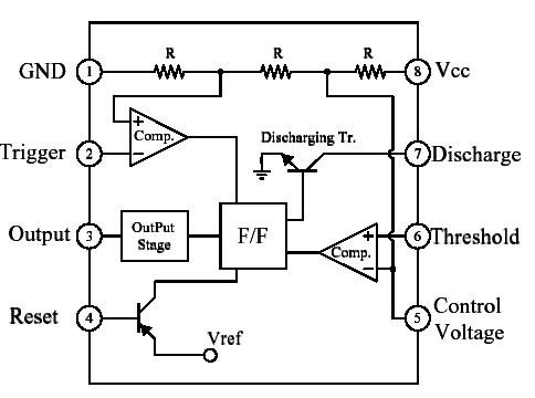
A typical 555 IC block diagram is as shown below.


Monostable Operation

Figure below shows the monostable operation of a 555 IC.


In this mode, the device generates a fixed pulse whenever the trigger voltage falls below Vcc/3. When the trigger pulse voltage applied to pin 2 falls below Vcc/3 while the its output is low, its internal flip-flop turns the discharging transistor Tr off and causes the output to become high by charging the external capacitor C1 and setting the flip-flop output at the same instant. The voltage across the external capacitor C1, VC1 increases exponentially with the time constant T=RA*C1 and reaches 2Vcc/3 at td=1.1RA*C1. Hence, capacitor C1 is charged through resistor RA. The greater the time constant RA*C1, the longer it takes for the VC1 to reach 2Vcc/3. In other words, the time constant RA*C1 controls the output pulse width. When the applied voltage to the capacitor C1 reaches 2Vcc/3, the comparator on the trigger terminal resets the flip-flop, turning the discharging transistor Tr on. At this time, C1 begins to discharge and its output goes to low.

Astable Operation


An astable operation is achieved by configuring the circuit as shown above. In the astable operation, the trigger terminal and the threshold terminal are connected so that a self-trigger is formed, operating as a multivibrator. When its output is high, its internal discharging transistor Tr turns off and the VC1 increases by exponential function with the time constant (RA+RB)*C. When the VC1, or the threshold voltage, reaches 2Vcc/3, the comparator output on the trigger terminal becomes high, resetting the F/F and causing its output to become low. This in turn turns on the discharging transistor Tr and the C1 discharges through the discharging channel formed by RB and the discharging transistor Tr. When the VC1 falls below Vcc/3, the comparator output on the trigger terminal becomes high and the timer output becomes high again. The discharging transistor Tr turns off and the VC1 rises again. The frequency of oscillation is given as below.

LOAD MATCHER

Most audio circuits transfer their maximum power at minimum distortion only when the output impedance is matched to the load impedance. But it is often necessary to connect equipment of differing impedances. For example, how do you correct an amplifier with a 600 ohm output into an amplifier with a 50 ohm input? Usually, if the 50 ohm input is connected across the amplifier with a 600 ohm output, the excessive loading caused by 50 ohms will sharply reduce the output of the 600 ohm amplifier, and will generally increase the distortion sharply.


A minimum loss pad is the device used to match a high impedance to a low impedance. Though there is always a signal level loss through a pad, the circuit shown provides the absolute minimum loss that can be obtained while providing a precise match. If the resistance values work out to odd values, such as 134 ohms, use the closest standard value. Though 5 percent tolerance resistors are suggested, almost as good performance will be obtained with 10 percent resistors.

REMOTE SPEAKER SETUP

Even if your hi-fi amplifier does not have output terminals for remote speakers, it is easy enough to add them without complex switching equipment. With few exceptions, modern solid-state amplifiers have no output transformers and automatically match any speaker impedance between 4 and 16 ohms. The only important consideration is that the total impedance connected to the left and/or right speaker output is never less than 4 ohms, or the amplifier will attempt to deliver so much power output, the output transistors will self-destruct. If your main speakers have an impedance of 8 or 16 ohms, simply add remote speakers as shown :


Switch S1 turns the remote speaker on and off. Since transistor amplifiers usually put out more power at 4 ohms than at 8 or 16 ohms, adding the extra speakers does not substantially reduce the volume at the main speakers because the amplifier sees a lower impedance load and attempts to drive more power output into the combined speaker load. If your speakers are 4 ohms, and you plan to use 4 ohm remote speakers use the circuit modification shown. Switching in the remote speaker will result in the main and remote speakers being series connected for a total load of 8 ohms.

HOW TO MAKE A TAN TIMER

This timer was designed for people wanting to get tanned but at the same time wishing to avoid an excessive exposure to sunlight.

A Rotary Switch sets the timer according to six classified Photo-types (see table).

A Photo resistor extends the preset time value according to sunlight brightness (see table).

When preset time ends, the beeper emits an intermittent signal and, to stop it, a complete switch-off of the circuit via SW2 is necessary.

Photo-type Features Exposure time
I & children Light-eyed, red-haired, light complexion, freckly 20 to 33 minutes
II Light-eyed, fair-haired, light complexion 28 to 47 minutes
III Light or brown-eyed, fair or brown-haired, light or slightly dark complexion 40 to 67 minutes
IV Dark-eyed, brown-haired, dark complexion 52 to 87 minutes
V Dark-eyed, dark-haired, olive complexion 88 to 147 minutes
VI The darkest of all 136 to 227 minutes
Note that pregnant women belong to Photo-type I


Components Used

R1_____________47K   1/4W Resistor
R2______________1M 1/4W Resistor
R3,R5_________120K 1/4W Resistors
R4____________Photo resistor (any type)

C1,C3__________10µF 25V Electrolytic Capacitors
C2____________220nF 63V Polyester Capacitor

D1,D2________1N4148 75V 150mA Diodes

IC1____________4060 14 stage ripple counter and oscillator IC
IC2____________4017 Decade counter with 10 decoded outputs IC

Q1____________BC337 45V 800mA NPN Transistor
SW1___________2 poles 6 ways Rotary Switch (see notes)
SW2___________SPST Slider Switch

BZ1___________Piezo sounder (incorporating 3KHz oscillator)

B1____________3V Battery (two 1.5V AA or AAA cells in series etc.)

NOTES

  • Needing only one time set suitable for your own skin type, the rotary switch can be replaced by hard-wired links.

  • A DIP-Switch can be used in place of the rotary type. Please pay attention to use only one switch at a time when the device is off, or the ICs could be damaged.

CB SNIFFER PROBE


It’s often difficult if not impossible to detect RF in mini-power RF circuits such as used in walkie-talkies; generally, service grade test equipment just isn’t sensitive enough. Next time you are working on a CB walkie-talkie and can’t tell if a lower power RF amplifier is working, just throw together a CB Sniffer Probe from remains of the old junk box. Better yet, why not be prepared in advance because all new components will cost less than $10. A small plastic rod about 6 inches long, cemented to L1, will allow you to se the sniffer as a probe. To align, place the sniffer near the antenna of a known good walkie-talkie, key the transmitter, and using an insulated alignment screwdriver adjust trimmer capacitor C1 for maximum brilliance of neon lamp l1.

Parts List For CB Sniffer Probe

C1
– 5 to 30 pF trimmer capacitor

l1 – NE-2 neon lamp

L1 - RF choke, ohmite Z-144 or equiv.

Sunday, December 27, 2009

HOW TO MAKE AN INFRARED SWITCH FOR THE PROJECT?-BIOMEDICAL ELECTRONICS PROJECTS

DESCRIPTION

This is a single channel (on / off) universal switch that may be used with any Infra Red remote control using 36-38kHz. (This is a very common remote handset frequency). In place of IR1 a TSOP1738 receiver may be used.

ir_switch
Notes

Any "button" of any remote control may be used to work this universal switch. The button must be pressed for about one and a half seconds (determined by R3 and C2) before the relay will operate. The circuit will remain in this state (latched) until reset. To reset, any button is pressed on the remote handset and held for a short duration.
For example, if you were watching TV, you could press and hold any button on the TV remote to trigger the circuit. In order not to change channel, you could press the button of the channel you are watching. You can connect anything to the relay, for example a lamp, but make sure that the relay contacts can handle the rated voltage and current.

Circuit Operation:
IC1 is an Infra Red module. IR modulated pulses are received and buffered by this IC. It has a standard TTL output, the output with no signal is held high by R1. A replacement for IR1 is the common TSOP1738 IR reciver. One gate of a CMOS inverter drives LED1 as a visible switching aid. Another gate buffers the signal and applies it to the time constant circuit, comprising R3,C2,R4 and D1. C2 charges via R3, and discharges via R4, D1 prevents quick discharge via the low output impedance of the CMOS buffer. If using a TSOP1738 then increase R4 to 470k.

The time taken to charge a capacitor is the product of resistance and capacitance, more commonly known as the RC time constant. At one RC a capacitor will only charge to 63% of the supply voltage. It takes 5 RC's for a capacitor to reach 99% charge. In this circuit the capacitor charge has to reach the logic threshold of the CMOS invertor. As the power supply is 5 Volts, the input threshold is around 3.6V, which takes about 3RC's or about 1.5 seconds. Once reached the inventor triggers the 555 timer and operates the flip flop. A simulation of received pulses, filtering and output pulse is shown below. Note that this is not from the actual circuit ( in which case the reconstructed pulse would be high for the duration of the 555 monostable) but only a spice simulation.

irsw_pulse

The pulses are further buffered and contain "jaggered edges" as shown above. These edges are produced by the modulated IR data, and have to be removed. This is achieved using a 555 timer wired as a monostable, IC3, having an output pulse duration R5, C4. A clean output pulse is produced to activate the bistable latch, IC4. This is a D type flip flop, built with a TTL 7474 series IC and configured as a bistable. Any version of the 7474 may be used, i.e. schottky 74LS74, high speed 74HCT74 etc. The input is applied to the clock pin, the inverted output fed back to the data input and clear and preset lines are tied to ground. For every pulse the relay will operate and latch, the next pulse will turn off the relay and so on. Note that quick turn on and off of the relay is not possible. The output pulse is set at about 2.4 seconds. and input delay by R3, C2 set about 1.5 seconds.

Parts List:
R1 3k3
R2 1k
R3 22k
R4 220k or 470k if using a TSOP1738
R5 1M
R6 3k3
B1 12 V
D1 1N4148
D2 1N4003
Q1 B109
LED1 CQX35A
IC1 IR1 available from Harrison Electronics or TSOP1838 or similar
IC2 4049
IC3 CA555
IC4 SN74HCT74 or SN74LS74
IC5 LM7805
Relay 12 Volt coil with changeover contact
C1 100u
C2 22u
C3 100n
C4 2u2
Reblog this post [with Zemanta]

HOW TO MAKE A METAL DETECTOR?-ELECTRONICS PROJECT

ABOUT

A single chip metal detecor with a range of a few inches. This is useful for decting nails or screws in walls and floors, or for locating buried mains cable.

CIRCUIT DIAGRAM

metaldetector

HOW TO MAKE INFRARED HEART PULSE MONITOR?-BIOMEDICAL PROJECTS


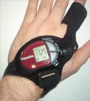
[caption id="" align="aligncenter" width="300" caption="Image via Wikipedia"]Photo of a strapless heart rate monitor[/caption]


I HAVE MADE A CIRCUIT ON HEART PULSE MONITOR

This circuit is given at the bottom

ABSTRACT FROM A PATENT ON HEART PULSE MONITOR

The invention herein described is intended to provide the user with a reliable heart rate monitor that is a completely self contained unit and is capable of providing accurate readings while the wearer is moving about. The use of piezoelectric sensing elements eliminates the power drain caused by LEDs and similar devices. The sensing element mounting means disclosed herein is devised to greatly reduce the noise introduced into the pulse signal by body motion. The use of optical sensors in a staring mode and optical sensors in a pulsed mode is also presented. The effects of noise are further reduced by employing digital signal processing algorithms to find the heart pulse intermixed with noise signals and present the heart pulse rate in beats per minute on a display. The resulting device permits the visual monitoring of the heart pulse rate in a human body in a consistent, error-free manner.

DOWNLOAD THIS PATENT FROM HERE

About the heart pulse monitor circuit

DOWNLOAD THE CIRCUIT DIAGRAM

THIS CIRCUIT DIAGRAM IS SELF EXPLANATORY

IF ANYONE NEEDS HELP THEN CONTACT THE ADMINISTRATOR
Reblog this post [with Zemanta]

Thursday, December 24, 2009

MAKE YOUR OWN EEG DEVICE-BIOMEDICAL PROJECTS

Overview


An EEG signal is usually acquired through silver-chloride covered electrodes, though sometimes other materials like pure silver, tin, steel or gold are used. The signal amplitude is only a few microvolt and needs to be amplified several thousand times before it can be captured. Because it is faint, the signal can very easily drown in noise, particularily 50/60Hz hum from the mains which is transmitted capacitively (i.e by an electric field) from the wiring in your house.

To handle this, the signal is first amplified by a high quality instrumentation amplifier, which measures the voltage difference between two locations on the scalp. In the example in the previous section, we used C3 and P3. This ensures that a large percentage of the mains hum never enters the system, because the level of the mains hum on those two locations is essentially the same.

Afterwards the signal strength is increased further by normal amplifiers, and passed through a low-pass filter which minimizes distortion caused by so-called aliasing that may occur when the signal is converted to digital samples.

Below is the block diagram of one EEG amplifier channel, and the Right-leg driver (DRL-circuit).


amp_block_diagramSimplified block diagram of the ModularEEG amplifier

Some parts are not included here. The schematic gives you all the details if you are interested.

The EEG signal is picked up by the two topmost electrodes and passed through the protection circut. It serves two purposes: First, it protects the circuitry from electrostatic discharge (ESD) and second it protects the user from failing circuitry. In theory at least.

Leaving the protection circuit, the signal enters the instrumentation amplifier where it is amplified 12 times. After that, the signal is amplified about 40 times in a second amplifier stage. You can't see it in the diagram, but there is a reason for splitting the amplification into two steps like this. Between the two stages there is a high-pass filter which removes DC-voltage offsets.

Some electrode materials, such as gold or steel, are polarizable. This means that electric charge can accumulate on the surface of the electrode, building up a relatively large DC-voltage, sometimes several hundred millivolts if you are unlucky. In theory, you would amplify a 200mV signal 480 and get a 96 volt output. In reality, the circuitry can handle about 2.5V so the output signal would be stuck at at a maximally high or low level, usually +/- 2.5V and not contain any EEG. The highpass filter tries to solve this problem.

Finally, the signal is amplified 16 times more and lowpass filtered. The filtering is done to prevent aliasing effects later on, when the signal is digitized.

Below the signal amplifiers, and the filter, sits a third amplifier pointing the other way, seemingly sending a signal to the user. This is the right-leg driver. It is named like this for historical reasons. The driver is, and was, previously only used by ECG meters, which measures the electrical activity in the heart. During ECG sessions, the driver (also abbreviated DRL, for Driven Right Leg) is attached to the right leg, as far away from the heart as possible.

The purpose of the DRL is to reduce common-mode signals such as 50/60Hz mains hum, by cancelling them out. It replaces a ground electrode which older EEG designs use, and can attenuate mains hum up to 100 times more than the instrumentation amplifier can do by itself.

After the filtering, the signal is ready for acquisition by the analog-to-digital converter which in our case is located inside a microcontroller. The microcontroller sends the digitized EEG to a PC via a standard serial cable. To protect the user from electrical faults, the EEG device is electrically isolated from the PC and external power sources. The block diagram below shows this.mcu_block_diagramDOWNLOAD MORE INFORMATION ABOUT THE PROJECT FROM THE LINKS BELOW

LINK1

Reblog this post [with Zemanta]

ELECTRONICS COMPONENTS SHOPS IN MUMBAI

Motors:
1. Mechtex - Mulund, Mumbai

2. Chip Components - Lamington road, Mumbai
Telefax: 2389 5667
Telephone: 56390468 / 56587005

3. EMAAR IMPEX P.LTD. (analog ICs, micros etc)
16A/2, Hanuman Terrace, Tara Temple Lane,
Lamington Road, Mumbai-400 007
Tel : +91-22-23854163
Fax: +91-22-23894197
http:www.emaarindia.com/

4. ORIOLE INDIA (LCDs etc)

HEAD OFFICE (MUMBAI) : 4, Kurla Industrial Estate, Narayan Nagar, Ghatkopar (W),
Mumbai-400 086. * Tel.: 91 22-2509 4241 - 46 * Fax : 91 22-2511 5810
BANGALORE (BRANCH ) : No. 5 & 6, 2nd Floor, 34, Renuka Complex, New Tippasandra Main Road, Bangalore-560 075. * Tel.: 91 80-2520 2816 * Fax : 91 80-2529 1433
NEW DELHI (BRANCH) : 116, Vardhaman Tower, Preet Vihar Community Centre,
New Delhi-110 092. * Tel. : 91 11-2245 4525 * Fax : 91 11-2245 8352
E-mail : sales@orioleindia.com
http:
www.orioleindia.com/

5. Pulraj Electronics Pvt. Ltd.
Regd Office : 4/A Shivalaya, Govandi Road, Chembur, Mumbai 400071
e-mail: pulraj@vsnl.com
for SIMCOM brand Industrial GSM Mobile / Modem (Rs.3,700/-)

6. APlus India (Check electronic magazine for address details)
for cheapest range of RF modules in Mumbai Market. Starts at Rs.350/- a pair for ASK/OOK

7. Rajkamal (RK) Electronic
48 - 50 Janardhan Bldg. shop No. 2, Proctor Road, Grant Road (E), Mumbai - 400007
Tel: 23820147 / 23864864.
Shop where you can get genuine audio IC's at a very good price in LR (Lamington Road) You also get all
different type of CODEC boards with him. He deals in Audio / Video spares.

8. Niki Semiconductors
Shop No. 1A, Ground Floor, Pushpant Nivas, 3 Chunam Lane, Lamington Road, Mumbai - 400007.
Tel. : 23884628, 5658 6112. E-mail: nikisemiconductors@mtnl.net.in
This guy deals in difficult to get EEPROM's (Windowed) , some Zif Sockets are easy buy , and also offers
programing facility for MCU's, and EEPROM. He also has some programs for Running light effect, TV Tunner
EEPROM, Some very old Mother Board BIOS dump , etc.

9. Hi-Tech Electronics Components
54/A, Jyoti Estate, Proctor Road, Grant Road (E) , Mumbai - 400007.
Tel. 3870106 / 389 2567 e-mail : tech_hi@vsnl.com
they deal in Industrial Electronic Components and you can find some Obsolete RF Prescalar with him, he
also NE612 and MC13135 IC's with him.

10. Bombay electronics
13-B, Shamrao Vithal marg, Off Lamington road, Mumbai - 400007.
Tel: 23885654 E-mail: paramjit_chandock@yahoo.com
They deal in AC & DC Gear motors, stepper, servo & micro motors, tyres and chasis too

Sunday, December 20, 2009

HOW TO MAKE A WIRELESS ELECTROCARDIOGRAM(ECG) MONITOR-BIOMEDICAL PROJECTS


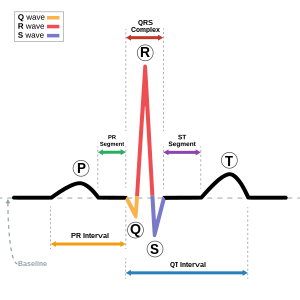
[caption id="" align="aligncenter" width="300" caption="Image via Wikipedia"]Schematic diagram of normal sinus rhythm for a...[/caption]


Introduction

The electrocardiogram (ECG or EKG) is a noninvasive test used to measure the electrical activity of the heart. An ECG can be used to measure the rate and regularity of heartbeats, the position of the chambers, the presence of any damage to the heart and the effects of drugs and devices used to regulate the heart. This procedure is very useful for monitoring people with heart disease or to provide diagnosis when someone has chest pains or palpitations.


Leads are placed on the body in several pre-determined locations, usually the extremities or the front of the chest, to provide information about heart conditions. For our final project, we implemented a wireless electrocardiogram monitor.


The following figure describes the overall high-level design for our ECG monitor:

High-Level

Three leads are placed on the subject --usually one on each side of the chest and on the lower abdomen. This signal is sent to the amplifier where it is amplified by a factor of one thousand. The signal is then sent to the voltage to frequency converter (VFC), which converts the signal to a frequency so that it can be transmitted. Since we desired the amplifier, VFC and transmitter to operate using only a single 9 V battery, a separate source splitter circuit was used to provide the proper voltage to each of the components.


Once the signal is received using the radio receiver, a voltage summer is used to add an offset voltage of approximately 800 mV to the signal in order to make the signal entirely positive. This signal is then amplified by a factor of three so that its maximum value exceeds the threshold of the required voltage for the frequency to voltage converter (FVC). After the signal is passed through the FVC, the output signal is displayed on an oscilloscope.


Hardware

The following schematic shows the amplifier section of the circuit:

DOWNLOAD THE SCHEMATIC

With the reference lead of the the subject placed to ground, each of the input chest leads is sent to an input of the INA121 instrumentation amplifier. Using a 4.7k resistor, a gain of 11.7 results from this stage. Following the instrumentation amp, the signal is passed through two 10 uF capacitors, placed back to back. The capacitors are used to prevent baseline drift in the ECG signal. Putting two directional capacitors back-to-back forms a bi-directional capacitor. A time constant of 0.5 second was chosen to approximate the frequency of a standard ECG signal (a resistor of 100k can be connected to ground after the capacitor in order to make a time constant of 0.5 sec, but we found that this resistive element is unnecessary). This section is followed by two inverting amplifiers each with a gain of ten. The total gain of this part of the circuit is approximately equal to one thousand.


The following schematic, obtained from the LM231 data sheet, shows the VFC circuit used in our monitor:


equ1


DOWNLOAD SCHEMATIC1


V_logic is connected to the power supply Vs and all ground are connected to the negative terminal of the battery. Fout is a square wave of varying frequency with a maximum amplitude of Vs. A voltage divider is needed (200k and 10k variable resistor connected in series) is needed at pin 3 to scale the voltage down to around 20 -50 mV.


The output of the voltage divider is connected to the input of the transmitter shown in the circuit diagram below.


Please note: We added everything on this schematics except for the 22k and the offset adjust. We neglected those two elements completely.


The following schematic describes the the source-splitting and transmitter section of our project:source-_trans


The source-splitting amplifier allows three different potential reference: + 4.5V, -4.5V and Ground. Since the BA1404 can only have +3V as its power supply, we used two diodes to create a total drop of 1.4V and this allows the transmitter to function properly. Another advantage to this setup is that every elements on this circuit can be powered off a signal 9V battery. Although not noted on this schematics, one should know that the input to the transmitter should be on the order of mV (5 - 50mV). Implementing a variable voltage divider to the input is very important. The nice thing about this setup is that one does not need an DC offset circuitry to adjust ECG signal from the output of the amplifier. Since our VFC is powered between -4.5V and +4.5V, it has a 4.5V offset already. If the ECG signal is centered at 0V with a swing from -0.5 to +0.5V, then the VFC sees it as 3.5V to 4.5V swing. It is important to know that VFC cannot have negative voltage as its input. Furthermore, making an inductor at the tunable FM transmitter range is a painstaking process. We found that by turning a wire 4 times around the pen allows the signal to be transmitted at 90 MHz.


Receiver Circuitry:


The following schematic shows the voltage summer and amplifier section of the project:


Summing Amplifier


This section consists os a summing amplifier with a gain of one cascaded with an inverting amplifier with a gain of approximately two. The summer takes the input obtained from the receiver (a FM radio tuned at approximately 90 MHz) and adds it to a constant voltage obtained using a simple voltage divider. This signal is then sent to an inverting amplifier which provides a gain of two and inverts the signal after it has been inverted by the summing amplifier. The reason we amplified the signal is due to the fact that FVC (LM231) needs at least a 2V peak-to-peak amplitude. The signal coming from the radio receiver has a peak-to-peak amplitude around 500 mV. Increasing the volume will normally increase the signal amplitude but it will also decrease the signal-to-noise (SNR) ratio. The amplifier we designed at the receiving end increase the signal to at least 5V of peak-to-peak amplitude, which is sufficient for FVC conversion.


The following figure shows the FVC circuit, also obtained from the LM231 data sheet:


equ2


Equation used to calculated the voltage output due to the frequency responseFVC


Results


One of the most difficult parts about this project is setting up the VFC (Voltage-to-Frequency) and FVC (Frequency-to-Voltage). Through many experimentations, we found out that the VFC can not convert a signal varying more than 16 Hz into pulse train. For example, when we fed in a 100 Hz sine wave, we were getting a constant square as the output (thus a constant DC voltage). This could be a potential problem for ECG transmission since the QRS peak can occur as fast as 20 to 50 Hz. However, when we fed in square waves of varying frequency into the FVC, we could get a varying DC voltage as expected. This is probably the reason why we could not receive a nice-looking ECG waveform on the receiving end. Also, we believe that the signal was attenuated during the transmission process. We had a difficult time receiving a nice looking square wave from the FM radio receive. However, we were able to fix that problem by increasing the volume on the radio to create better rising and falling edges for the FVC. Finally, we noticed that our transmission range is about 10 feet, which is not very useful for a wireless ECG. The pictures below demonstrate our final result:


114-1431_IMG


Transmitter Section (this includes, pre-amp, source-splitting, FM transmitter and VFC).


IMAGES OF CIRCUIT


1,


2,


3,


4,


5,


6,


REFERENCES


LM231.pdf (VFC and FVC)


LM158.pdf (Operational Amplifier)


INA121.pdf (Instrumentation Amplifier)


http://www.medicinenet.com/Electrocardiogram_ECG_or_EKG/article.htm


http://www.nlm.nih.gov/medlineplus/ency/article/003868.htm
Reblog this post [with Zemanta]
Your Ad Here