Timer circuit has been used in many projects and there are basically 2 types that are used these days. One of them is the use of analog RC circuit where charging of the capacitor circuit determined the T(time) of the circuitry. This type of circuitry has larger tolerance and is used in applications where the T is not so critical as the T is affected by the tolerance of the RC components used.
The other is the use of crystal or ceramic resonators together with microprocessor, microcontroller or application specific integrated circuit that need higher precision T in the tolerance of up to 5 ppm (parts per million).
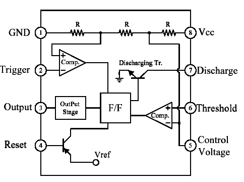
555 IC
One commonly used circuit is the 555 IC which is a highly stable controller capable of producing timing pulses. With a monostable operation, the T(time) delay is controlled by one external resistor and one capacitor. With an astable operation, the frequency and duty cycle are accurately controlled by two external resistors and one capacitor. The application of this integrated circuit is in the areas of PRECISION TIMING, PULSE GENERATION, TIMING DELAY GENERATION and SEQUENTIAL TIMING.
A typical 555 IC block diagram is as shown below.
Monostable Operation
Figure below shows the monostable operation of a 555 IC.

In this mode, the device generates a fixed pulse whenever the trigger voltage falls below Vcc/3. When the trigger pulse voltage applied to pin 2 falls below Vcc/3 while the its output is low, its internal flip-flop turns the discharging transistor Tr off and causes the output to become high by charging the external capacitor C1 and setting the flip-flop output at the same instant. The voltage across the external capacitor C1, VC1 increases exponentially with the time constant T=RA*C1 and reaches 2Vcc/3 at td=1.1RA*C1. Hence, capacitor C1 is charged through resistor RA. The greater the time constant RA*C1, the longer it takes for the VC1 to reach 2Vcc/3. In other words, the time constant RA*C1 controls the output pulse width. When the applied voltage to the capacitor C1 reaches 2Vcc/3, the comparator on the trigger terminal resets the flip-flop, turning the discharging transistor Tr on. At this time, C1 begins to discharge and its output goes to low.
Astable Operation

An astable operation is achieved by configuring the circuit as shown above. In the astable operation, the trigger terminal and the threshold terminal are connected so that a self-trigger is formed, operating as a multivibrator. When its output is high, its internal discharging transistor Tr turns off and the VC1 increases by exponential function with the time constant (RA+RB)*C. When the VC1, or the threshold voltage, reaches 2Vcc/3, the comparator output on the trigger terminal becomes high, resetting the F/F and causing its output to become low. This in turn turns on the discharging transistor Tr and the C1 discharges through the discharging channel formed by RB and the discharging transistor Tr. When the VC1 falls below Vcc/3, the comparator output on the trigger terminal becomes high and the timer output becomes high again. The discharging transistor Tr turns off and the VC1 rises again. The frequency of oscillation is given as below.


No comments:
Post a Comment